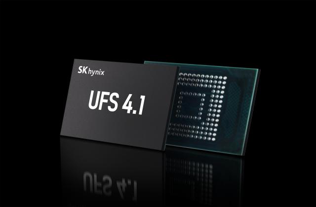
The company’s latest offering is a Universal Flash Storage (UFS) 4.1 solution built using its 321-layer 1-terabit Triple Level Cell (TLC) 4D NAND flash — the tallest NAND stack produced to date, according to SK hynix.
The new chip, the company said, is designed to meet the growing demand for fast and energy-efficient storage solutions capable of supporting stable on-device AI applications.
Compared with the previous generation built on 238-layer NAND, the new solution improves power efficiency by 7 percent and reduces thickness from 1 millimeter to 0.85 millimeters, enabling integration into increasingly thinner mobile devices.
These enhancements are seen as crucial as manufacturers seek to balance the performance demands of AI workloads with battery life constraints in mobile form factors.
The UFS 4.1 solution delivers sequential read speeds of up to 4,300 megabytes per second — the maximum supported under current UFS 4.1 specifications — and boasts improvements in random read and write speeds of 15 percent and 40 percent, respectively. SK hynix said this marks the highest performance among UFS 4.1 products currently available.
The company plans to offer the new storage chip in 512-gigabyte and 1-terabyte capacities for customer validation later this year, with mass production slated to begin in the first quarter of 2026.
The product is aimed at enhancing app responsiveness and reducing latency in data delivery — key requirements for AI-driven mobile user experiences.
“Following this product launch, we plan to complete development of consumer and data center SSDs based on the same 321-layer 4D NAND technology within the year,” said Ahn Hyun, Chief Development Officer at SK hynix. “Through this, we will build a product portfolio that enhances our competitiveness in AI-enabled NAND solutions and establish ourselves as a full-stack AI memory provider.”

Copyright ⓒ Aju Press All rights reserved.