S

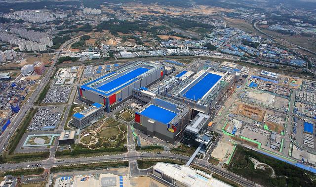
Samsung Electronics' production base in Pyeongtaek. [Courtesy of Samsung Electronics]
Samsung said it would boost its foundry capacity at the new production line at a production base in Pyeongtaek, about 60 kilometers (37 miles) south of Seoul, to meet growing global demand for cutting-edge extreme ultraviolet (EUV) solutions. The new foundry line is expected to be in full operation in the second half of 2021.
EUV chip manufacturing, also known as EUV lithography, is a technology using extreme ultraviolet light wavelengths to expose an ultra-thin electrical circuit.
The new line in Pyeongtaek will play a pivotal role as Samsung aims to expand the use of state-of-the-art process technologies across a myriad of current and next-generation applications, including 5G, high-performance computing and artificial intelligence, the company said in a statement on Thursday.
"This new production facility will expand Samsung's manufacturing capabilities for sub-5nm process and enable us to rapidly respond to the increasing demand for EUV-based solutions," Samsung's foundry business head Jung Eun-seung was quoted as saying. "This will enable us to continue to break new ground while driving robust growth for Samsung’s foundry business."
Samsung has added a new EUV-dedicated line in Hwaseong to its global foundry network. The mass production of the 5-nanometer EUV process in Hwaseong will begin in the second half of this year. With the Pyeongtaek line, Samsung would have seven foundry production lines in South Korea and the United States
Samsung, which is the world's largest smartphone and microchip producer, has revealed a massive investment worth 133 trillion won ($108 billion) by 2030 to strengthen its competitiveness in System LSI and foundry businesses, saying it aims to become the world leader in not only memory semiconductors but also logic chips.
LSI, also known as Large-Scale-Integration, is a chip-making process in which thousands of transistors are integrated or embedded onto a single silicon chip. Foundry refers to a semiconductor fabrication plant operation.
With next-generation technologies, Samsung is determined to achieve the top spot in system semiconductors by narrowing the gap with Taiwan Semiconductor Manufacturing Company (TSMC) through a battle of technical skills. The two companies are competing to grab the upper hand in the 5-nano process, which is the most difficult and ultra-fine process.
Samsung aims to produce 3-nano products by 2022 and upgrade its ultra-fine process by applying gate-all-around (GAA), a next-generation transistor structure. Its goal is to produce 3-nano-based products in 2022.
Copyright ⓒ Aju Press All rights reserved.


