SK hynix has begun construction of an advanced packaging production facility in Cheongju, North Chungcheong Province, as it moves to strengthen its position in the artificial intelligence memory market.
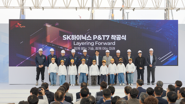
The company held a groundbreaking ceremony on the 22nd at a 230,000-square-meter (about 70,000-pyeong) site in the Cheongju Technopolis industrial complex for the new fab, named P&T7. SK hynix said the plant will have about 150,000 square meters (about 46,000 pyeong) of cleanroom space, combining roughly 60,000 square meters (about 18,000 pyeong) across three floors of process lines and about 90,000 square meters (about 28,000 pyeong) across seven floors of wafer test (WT) lines.
The company is targeting completion of the WT lines in October next year and completion of the wafer-level packaging (WLP) lines in February the following year.
P&T7 is a dedicated facility for advanced packaging, a key step for producing AI memory such as high-bandwidth memory (HBM). Packaging, part of the back-end semiconductor process, has gained importance as a way to overcome limits of chip miniaturization and improve performance and power efficiency.
SK hynix said it chose the site to maximize synergy with its existing Cheongju production base, including the operating M11, M12 and M15 fabs and the M15X fab now under construction, to improve logistics and operations. The company plans to link DRAM produced at M15X to P&T7 to complete final HBM products under an integrated production system.
SK hynix said P&T7 is more than an expansion of production capacity, calling it “the result of trust built together by the region and the company.” It added that it will work closely with the local community and aim to set “a successful milestone” for balanced national development.
* This article has been translated by AI.
Copyright ⓒ Aju Press All rights reserved.