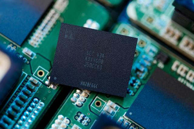
The new V-NAND utilizes innovative "channel hole etching" technology to achieve the highest layer count in the industry with a double-stack structure. The QLC variant boasts an unprecedented bit density, approximately 86 percent higher than its predecessor, by minimizing cell and peripheral circuit areas.
To maintain uniform cell characteristics across layers, Samsung employed "designed mold" technology, enhancing data retention performance by about 20 percent and improving product reliability. The company also introduced "predictive program" technology, boosting writing performance by 100 percent and data input/output speed by 60 percent compared to the previous QLC generation.
Power consumption has been significantly reduced through low-power design techniques, with read and write operations consuming approximately 30 percent and 50 percent less power, respectively.
"By successfully mass-producing 9th-generation QLC V-NAND just four months after 9th generation TLC, we have completed the latest lineup required by the high-performance, high-capacity SSD market for AI applications,” Han Seong-hoi, executive vice president of flash memory development, said.
Copyright ⓒ Aju Press All rights reserved.


