Samsung Electronics and SK Hynix have begun supplying samples of the seventh-generation High Bandwidth Memory (HBM4E) ahead of market expectations, shaking up the semiconductor back-end ecosystem. A fierce competition is emerging among domestic and global companies to dominate the hybrid bonder equipment market, a key component of next-generation packaging.
According to industry sources on June 22, the supply timeline for hybrid bonders from domestic semiconductor equipment manufacturers is expected to be significantly accelerated. The application of hybrid bonding technology starting with HBM4E is crucial for determining chip performance. Unlike traditional thermal compression (TC) bonders, hybrid bonders stack chips without micro bumps, reducing layer thickness while maximizing speed and current efficiency, making them essential for achieving high-performance HBM.
Hanmi Semiconductor plans to enter mass production of hybrid bonders as early as the second half of this year. This move is seen as a strategy to maintain leadership in the next-generation market by leveraging precision control technology accumulated in the TC bonder market.
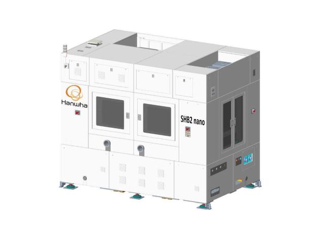
Hanwha Semitek aims to complete the development of its hybrid bonder within this year, collaborating with Dutch motion control specialist Prodrive. The company has shortened its original timeline by several months to enter the supply chain this year. Recently, it has been conducting quality tests on its hybrid bonding integrated cluster system, which includes its own equipment for aligning and bonding die and wafers, along with plasma activation and cleaning modules, at SK Hynix's facility.
Samsung's subsidiary Semes has also finalized a supply contract for hybrid bonders with full support from the group. Notably, it has developed wafer-to-wafer (W2W) technology, which has garnered attention. This method allows for the direct bonding of entire wafers, as opposed to the traditional die-to-wafer (D2W) process that stacks individual chips sequentially, significantly reducing the physical distance between chips. This results in thinner packaging while enhancing signal transmission speed.
Global companies focused on front-end processes are also accelerating their expansion into the back-end sector as they enter a generational transition phase. As the miniaturization of circuits on wafers reaches physical limits, the back-end processes of stacking and packaging chips are emerging as a new competitive advantage that influences memory performance.
Applied Materials has partnered with Dutch company VESI to launch the hybrid bonding cluster 'Kynex' as part of its market strategy. Having already secured Taiwan's TSMC as an ally, it has recently received a purchase order from key client SK Hynix for actual production line deployment.
An industry insider noted, "Hybrid bonders represent a high-level technology that transcends traditional TC bonding methods, fundamentally changing the packaging paradigm. HBM4E, along with the next-generation HBM5 market, will be a decisive factor in determining success, making the competition among companies to seize leadership more intense than ever."
* This article has been translated by AI.
Copyright ⓒ Aju Press All rights reserved.