

SEOUL, July 13 (AJP) - South Korean researchers have found a way to remove one of the biggest hidden bottlenecks inside computer chips, a discovery that could make future artificial intelligence processors faster and far less power-hungry.
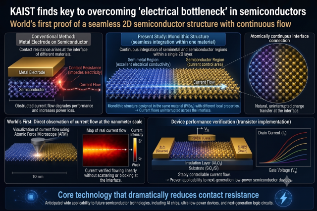
Every chip loses energy at the point where metal wiring meets the semiconductor material that does the actual computing. This so-called contact resistance works like a tollgate on a highway: electricity slows down, heat builds up, and power is wasted. The smaller the chips become, the worse the problem gets, which is why the industry regards it as one of the hardest obstacles to building the next generation of processors.
The Korea Advanced Institute of Science and Technology (KAIST) said Monday that a team led by materials science professor Hong Seung-bum, working with KAIST colleague Kang Ki-bum and Sungkyunkwan University professor Cho Sung-beom, had built a chip structure in which electricity flows across that troublesome boundary without any blockage, and observed it happening for the first time at the scale of a nanometer, one billionth of a meter.
The trick was to get rid of the boundary altogether. Instead of attaching a metal electrode on top of a semiconductor, as chipmakers have always done, the team used a single sheet of platinum diselenide, a material only one or two atoms thick. Within that one sheet, they created a region that conducts like a metal and a region that behaves like a semiconductor, joined seamlessly with no gap, glue, or residue in between. Because both regions belong to the same continuous material, current passes from one to the other as if driving on an uninterrupted road.
Using an atomic force microscope, an instrument that traces surfaces with a needle fine enough to map individual atoms, the researchers watched electric charge cross the junction. The current flowed straight through without stalling or bending, the first direct experimental proof that such a seamless interface does not resist the flow of electricity.
The team then went a step further and tested whether the structure could do real work. By applying an electric field to the semiconductor region, they switched the current on and off in a stable way, the basic operation of a transistor, the building block of every processor and memory chip.
The practical implications are significant. Contact resistance is a major reason data centers running AI models consume enormous amounts of electricity and generate so much heat. A chip architecture that eliminates the bottleneck could translate into AI processors that run faster on less power, longer battery life in phones and laptops, and ultra-low-power chips for sensors and wearable devices. The technique also gives chip designers a testing platform to evaluate electrode structures before committing them to production.
The work remains laboratory science for now, and the team plans to extend the method to other ultrathin materials in the same family before it can move toward commercial use.
"This is the first time anyone has directly observed current flowing across a two-dimensional semiconductor interface at the nanometer scale," Hong said. "Since we have experimentally proven that a seamless interface does not obstruct the flow of current, we expect it to serve as a core technology for solving contact resistance problems in a wide range of next-generation semiconductors."
KAIST doctoral candidate Kim Yeon-gyu, KAIST researcher Gyeon Min-seung and Sungkyunkwan University doctoral candidate Hong Ji-hoon were co-first authors of the study, which was published in the July 2026 issue of the materials science journal Matter.
(Reference Information)
Journal/Source: Matter
Title: Nanoscale imaging of charge transport across the semimetal-semiconductor interface in monolithic platinum diselenide
Link/DOI: https://doi.org/10.1016/j.matt.2026.102873

Copyright ⓒ Aju Press All rights reserved.