
SEOUL, August 13 (AJP) -SK hynix is set to break ground later this month on its $3.87 billion advanced semiconductor packaging plant in Indiana, the chipmaker’s first U.S. production base for packaging high-bandwidth memory used in artificial intelligence systems.
The West Lafayette project will also include an advanced packaging R&D facility and is scheduled to begin mass production in the second half of 2028.
According to industry sources on Thursday, the South Korean memory chipmaker has sent invitations to major customers and business partners for a formal groundbreaking ceremony scheduled for Aug. 27. Preliminary construction is already underway, with full-scale structural work expected to follow the ceremony.
Among the expected attendees are senior executives and representatives from major global technology companies, with particular attention on whether SK Group chairman Chey Tae-won and Nvidia CEO Jensen Huang will meet again.
SK hynix and Nvidia have been strengthening their cooperation in artificial intelligence (AI)-related sectors, including the supply of memory chips and graphics processing units for AI data centers. Chey and Huang have met several times in South Korea and the U.S. since last year to discuss the rapidly growing AI and semiconductor markets.
If Chey attends the ceremony, market attention is also likely to focus on whether he unveils plans for additional investment in the U.S. Chey recently said that SK hynix could consider building a memory chip manufacturing plant in the U.S. if key conditions are met.
The comments were seen as a response to the U.S. government's push for South Korean chipmakers to expand their production bases in the U.S., after U.S. Commerce Secretary Howard Lutnick repeatedly called on Samsung Electronics and SK hynix to increase memory chip production there.
SK hynix is investing US$3.87 billion in the West Lafayette facility on the campus of Purdue University as part of its strategy to build a more localized AI semiconductor supply chain and expand its U.S. operations.
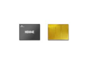
Once completed, it will be SK hynix's first advanced packaging and research and development facility on U.S. soil to produce high-bandwidth memory (HBM) chips for AI applications, with mass production targeted for the second half of 2028.
The project is also backed by U.S. government support, with the Commerce Department pledging up to US$458 million in direct funding under the CHIPS and Science Act, which aims to boost domestic semiconductor manufacturing, reduce reliance on foreign supply chains and support research in areas such as artificial intelligence and robotics.
AJP Takeaways:
- SK hynix will hold a groundbreaking ceremony for its advanced semiconductor packaging facility in West Lafayette, Indiana on Aug. 27, 2026.
- SK Group Chairman Chey Tae-won and Nvidia CEO Jensen Huang could attend the ceremony, drawing attention to their companies' growing cooperation in artificial intelligence and semiconductors.
- SK hynix is investing US$3.87 billion in the West Lafayette facility on the campus of Purdue University to expand its U.S. operations and build a more localized AI semiconductor supply chain.
- The facility will be SK hynix's first advanced packaging and research and development facility in the United States and is scheduled to begin mass production of high-bandwidth memory (HBM) chips for AI applications in the second half of 2028.
- The U.S. Department of Commerce has pledged up to US$458 million in direct funding under the CHIPS and Science Act to support the project and strengthen domestic semiconductor manufacturing.
The West Lafayette project will also include an advanced packaging R&D facility and is scheduled to begin mass production in the second half of 2028.
According to industry sources on Thursday, the South Korean memory chipmaker has sent invitations to major customers and business partners for a formal groundbreaking ceremony scheduled for Aug. 27. Preliminary construction is already underway, with full-scale structural work expected to follow the ceremony.
Among the expected attendees are senior executives and representatives from major global technology companies, with particular attention on whether SK Group chairman Chey Tae-won and Nvidia CEO Jensen Huang will meet again.
SK hynix and Nvidia have been strengthening their cooperation in artificial intelligence (AI)-related sectors, including the supply of memory chips and graphics processing units for AI data centers. Chey and Huang have met several times in South Korea and the U.S. since last year to discuss the rapidly growing AI and semiconductor markets.
If Chey attends the ceremony, market attention is also likely to focus on whether he unveils plans for additional investment in the U.S. Chey recently said that SK hynix could consider building a memory chip manufacturing plant in the U.S. if key conditions are met.
The comments were seen as a response to the U.S. government's push for South Korean chipmakers to expand their production bases in the U.S., after U.S. Commerce Secretary Howard Lutnick repeatedly called on Samsung Electronics and SK hynix to increase memory chip production there.
SK hynix is investing US$3.87 billion in the West Lafayette facility on the campus of Purdue University as part of its strategy to build a more localized AI semiconductor supply chain and expand its U.S. operations.
Once completed, it will be SK hynix's first advanced packaging and research and development facility on U.S. soil to produce high-bandwidth memory (HBM) chips for AI applications, with mass production targeted for the second half of 2028.
The project is also backed by U.S. government support, with the Commerce Department pledging up to US$458 million in direct funding under the CHIPS and Science Act, which aims to boost domestic semiconductor manufacturing, reduce reliance on foreign supply chains and support research in areas such as artificial intelligence and robotics.
AJP Takeaways:
- SK hynix will hold a groundbreaking ceremony for its advanced semiconductor packaging facility in West Lafayette, Indiana on Aug. 27, 2026.
- SK Group Chairman Chey Tae-won and Nvidia CEO Jensen Huang could attend the ceremony, drawing attention to their companies' growing cooperation in artificial intelligence and semiconductors.
- SK hynix is investing US$3.87 billion in the West Lafayette facility on the campus of Purdue University to expand its U.S. operations and build a more localized AI semiconductor supply chain.
- The facility will be SK hynix's first advanced packaging and research and development facility in the United States and is scheduled to begin mass production of high-bandwidth memory (HBM) chips for AI applications in the second half of 2028.
- The U.S. Department of Commerce has pledged up to US$458 million in direct funding under the CHIPS and Science Act to support the project and strengthen domestic semiconductor manufacturing.
Copyright ⓒ Aju Press All rights reserved.