

Journalist

Candice Kim김혜준
candicekim1121@ajupress.com
ReporterSamsung Electronics, SK hynix, LG Electronics, Olive Young, Musinsa & Semiconductor, K-Beauty
Candice Kim is a dedicated business and technology reporter specializing in the intersection of high-tech innovation and fast-paced consumer trends. Her core beats span the semiconductor, IT, cosmetics, and retail sectors, where she provides in-depth coverage of industry titans including Samsung Electronics, SK hynix, and LG Electronics, alongside leading consumer brands like Olive Young and Musinsa. Whether analyzing complex silicon supply chains or tracking the latest shifts in beauty and fashion retail, Candice is committed to delivering sharp, accurate reporting that keeps readers informed on the forces shaping today's most dynamic markets.
"Connecting the dots from silicon chips to consumer shifts."
Latest by Candice Kim
-
 SK hynix eyes near-80% margin as investors await bigger payouts SEOUL, October 26 (AJP) - SK hynix, South Korea’s leading supplier of memory crucial to artificial intelligence chips, is widely expected to deliver another earnings milestone this week with quarterly operating profit of about 77 trillion won ($58 billion) and a margin approaching 80 percent. The FnGuide consensus puts operating profit at about 77 trillion won on revenue of roughly 98 trillion won, translating into a staggering operating margin of about 79 percent for the quarter ended September. The profit forecast is about 27 percent above the previous quarterly record of 60.5 trillion won in April–June, 61 percent from 37.6 trillion won in the first quarter, with the operating margin reaching 76 percent. SK hynix releases its third-quarter results Wednesday. Its shares were trading 1.6 percent higher at 1,297,000 won early Monday, recovering from an intraday low of 1,190,000 won on Oct. 20 amid doubts over the sustainability of AI spending, but more than 56 percent below the June 22 intraday peak of 2,987,000 won. Investors are also watching for additional shareholder returns, including a possible distribution of gains from the company’s stake in Japanese NAND flash memory maker Kioxia. SK hynix is considering paying out some of those gains in installments and may make the announcement during earnings call Wednesday. The company invested 395 billion yen in 2018 as part of a Bain Capital-led consortium that acquired Toshiba’s memory business, now Kioxia, for 2 trillion yen. It recovered about 4.12 trillion won from partial disposals in the first quarter. Given the Japanese chipmaker's second-quarter gains at around 20 trillion won, this year’s dividends could substantially exceed last year’s total of 2.1 trillion won. The potential payout would follow a 40 trillion won share buyback announced in August. Purchases were completed on Oct. 21, about a month ahead of the original Nov. 19 deadline, with the acquired shares earmarked for cancellation. SK hynix also strengthened its shareholder-return framework in August, targeting more than 50 percent of cumulative free cash flow for 2025–2027 through dividends, buybacks and share cancellations. That replaced its previous policy of returning up to 50 percent. Samsung Electronics will follow with its detailed third-quarter results Thursday, including a breakdown across its semiconductor, smartphone and home-appliance businesses. Samsung projected operating profit of 107.4 trillion won on revenue of 195 trillion won in preliminary guidance released Oct. 8. Its shares were down 0.7 percent at 214,000 won early Monday. 2026-10-26 10:02:50
 -
 Apple's first foldable rekindles iPhone fever in South Korea SEOUL, October 23 (AJP) - Apple’s first foldable has finally arrived in South Korea, rekindling iPhone fans’ fading affection and drawing hundreds to stores to get their hands on the real thing — despite a price tag of more than 3 million won. Outside Apple’s flagship store in Seoul’s Garosugil shopping district on Friday, three people who appeared to be strangers exchanged polite bows before one handed another a box containing the new iPhone Duo. The brief encounter, apparently a purchase on someone else’s behalf or a resale transaction, offered a glimpse of the demand for Apple’s first foldable smartphone as it went on sale in South Korea after nearly a decade of speculation. Those collecting their phones inside were among the fortunate buyers who had secured preorders before they sold out in a minute. Customers lined up early to collect their devices at Apple Garosugil. Similar scenes unfolded at Apple’s Myeongdong store, where more than 100 people gathered ahead of opening. “Some customers lined up early because they wanted to pick up their phones and unbox them right away,” one shop staff said. Walk-in purchases were unavailable. Canceled orders went back into the online inventory, the staff explained. Apple’s website showed a Jan. 22 delivery date for orders placed Friday — a three-month wait. Some foreign visitors also tried their luck. “There were quite a few foreign customers in the queue this morning, but some left because they couldn’t buy one on the spot,” the staff said. Foreign-issued payment cards could be used for online purchases, but customers without an eligible local address could not complete the pickup process. For some shoppers who had switched from iPhones to Samsung’s refined foldables, the Duo offered a reason to consider flipping back. “One customer brought in Samsung’s latest Fold and compared the two side by side,” the staff said. “They liked the Duo and ended up ordering one.” That kind of exchange could worry Samsung as Apple challenges its hard-won foothold in foldables. It reigns for now. This year's series Galaxy Z Fold8, Fold8 Ultra and Flip8 recorded a combined 1.44 million preorders in South Korea over seven days in late July and early August, up 39 percent from the previous generation. The Fold8 accounted for about 70 percent of those orders. Demand outstripped initial supplies for some Fold8 models, prompting Samsung to extend its preorder activation period through Aug. 31. Price remains a dividing line. The iPhone Duo starts at 3.29 million won for the 256GB model and reaches 5.09 million won for the 2TB version. Samsung’s 256GB Galaxy Z Fold8 starts at 2.28 million won — roughly 1 million won cheaper than Apple’s entry model. Inside the Garosugil store, employees emphasized that the Duo was designed for customers with different priorities from buyers of conventional flagship phones. One employee pointed to its 7.6-inch foldable inner display and matte, nano-textured finish, which reduces reflections. “The screen itself has a matte finish. It’s not a film,” the employee said, explaining that the design was intended to make content easier to see from different angles. The larger display could particularly appeal to designers and video creators who need more room to view their work and use multiple applications, the employee suggested. Another staff member drew a distinction between the Duo and Apple’s recently released iPhone 18 lineup. Customers who prioritize photography might prefer a conventional iPhone, the employee said. Those accustomed to working or multitasking on an iPad might find the Duo more useful. The product has been a long time coming. Reports of Apple’s interest in foldable displays date back to at least 2016, when patent filings and industry speculation raised the prospect of an iPhone that could bend in half. Samsung launched its first Galaxy Fold in 2019. Apple waited another seven years to enter the market. One industry source familiar with Apple’s approach attributed the lengthy development partly to its insistence on refining products before releasing them. “Apple is almost obsessive about perfection,” the source said, pointing to its attention to detail in both retail stores and product engineering. That remains an industry interpretation rather than Apple’s official explanation for its development timeline. Longtime fans, however, appear pleased enough to wait three months — or pay a resale premium on top of an already hefty price tag. 2026-10-23 14:23:38
 -
 SK drops Solidigm IPO amid regulatory and shareholder pressure SEOUL, October 23 (AJP) - SK hynix has dropped plans to list its U.S. NAND flash subsidiary Solidigm amid pressure from South Korean regulators and minority shareholders over the potential erosion of shareholder value. “Solidigm, our overseas subsidiary, has reviewed various financing options to expand production capacity and strengthen its competitiveness. However, after comprehensively considering capital market conditions and other factors, it has decided to discontinue its review of pre-IPO fundraising and an initial public offering,” the company said in a regulatory filing Friday. The disclosure followed earlier filings responding to an August media report that Solidigm was considering a pre-IPO fundraising round of about 5 trillion won. The retreat came just a day after Financial Services Commission Chairman Lee Eog-weon confirmed that a separate U.S. listing of Solidigm would fall under South Korea’s rules governing the listing of subsidiaries of publicly traded companies. Asked at a parliamentary audit whether he agreed with the Financial Supervisory Service governor’s assessment that the proposed IPO constituted a parent-subsidiary listing, Lee replied: “Yes. It is subject to the guidelines.” “SK Square and SK hynix must fulfill the five obligations imposed on parent companies based on their duty of loyalty to shareholders,” he added. The requirements include assessing the impact on shareholders, devising protections, consulting investors, obtaining a board decision and disclosing the process. The obligations also apply when a subsidiary seeks to list overseas. Shareholder opposition had intensified as investors questioned whether a standalone listing would dilute SK hynix’s interest in the business and deepen the discount applied to its remaining stake. SK hynix had about 3.46 million small shareholders holding 67.98 percent of its outstanding shares at the end of June, according to its half-year report. Shareholder group ACT called for a review of the proposed listing and the protections available to existing investors. The withdrawal also comes after a sharp reversal in the chipmaker’s shares on both sides of the Pacific. Its Seoul-listed stock closed Thursday at 1,223,000 won, down about 34.3 percent from 1,862,000 won on Sept. 25. Its Nasdaq-listed American depositary receipts, trading under the ticker SKHY, fell 8.07 percent Thursday to $131.69. That left them $17.31, or 11.6 percent, below their $149 offering price in July, when SK hynix raised about $26.5 billion in its U.S. share sale. Solidigm’s proposed listing had promised a substantial new source of capital. Solidigm emerged from SK hynix’s roughly $9 billion acquisition of Intel’s NAND flash and solid-state drive business, announced in 2020. The U.S. company began operating under the Solidigm name in 2021 and supplies high-capacity storage drives for servers, cloud computing and AI data centers. After years of losses, its return to profitability made the question of who would benefit from its growth more contentious. The ownership chain runs from SK Inc. through SK Square and SK hynix to AI Company, which holds Solidigm. SK Inc., SK Innovation and SK Telecom have also committed capital to AI Company, creating additional ownership interests alongside SK hynix’s. The Korea Corporate Governance Forum argued that this structure could allow part of the increase in Solidigm’s value to accrue to other group companies in which Chairman Chey Tae-won has a larger economic interest. It called for the listing to be halted, citing the potential disadvantage to SK hynix shareholders. SK hynix said Friday that Solidigm’s growth prospects and investment needs had not changed. Rather, recent capital-market conditions and share-price movements warranted reconsidering whether an IPO was the best option for the company and its existing shareholders. It said it would continue examining the timing, scale and financing of investments needed to expand Solidigm’s capacity and competitiveness. 2026-10-23 08:13:58
 -
 Samsung's Lee visits UAE power plant SEOUL, October 22 (AJP) - Samsung Electronics Chairman Lee Jae-yong visited a gas-fired power plant construction site in Abu Dhabi on Wednesday as the South Korean conglomerate explores opportunities in AI data centers and energy infrastructure in the Middle East. Lee inspected construction progress and safety measures at the Al Dhafra power plant, which Samsung C&T is building in a consortium with local contractor Trojan General Contracting, the company said Thursday. During the visit, Lee met executives from Samsung C&T and Samsung E&A to discuss regional business conditions and potential expansion into new projects. Samsung has an established presence in the UAE through projects including the Barakah nuclear power plant and oil, gas and petrochemical facilities. The group is exploring further opportunities in power infrastructure as electricity demand rises alongside industrial development and AI-related investment. Lee also met employees working in the region. Earlier this month, he sent letters and gifts to 730 Samsung employees stationed across nine Middle Eastern countries and their families, citing concerns over their safety amid regional tensions. 2026-10-22 16:27:19
 -
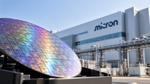 Korean chip bonuses spill over to competition SEOUL, October 22 (AJP) - Chipmakers in South Korea and Taiwan keep a civil distance despite cutthroat competition to advance chip technology and recruit talent. But the extraordinary AI chip windfall has turned heads in Taiwan’s cleanrooms as workers watch their Korean counterparts collect lavish rewards from the industry’s newfound riches. Union officials at U.S. memory chipmaker Micron Technology’s Taoyuan operation began a 24-hour warning strike Thursday, pressing for a permanent share of profits and drawing inspiration from compensation deals at Samsung Electronics and SK hynix. Eleven union officials began the action outside the plant at 9 a.m. after negotiations on Wednesday failed to resolve the dispute, Taiwan’s Liberty Times reported. The limited action should not be confused with a walkout by the plant’s entire workforce. The dispute adds another dimension to the rivalry among the world’s three leading memory chipmakers. Beyond technology and market share, the rewards negotiated by Korean workers are becoming benchmarks for employees at their American competitor. Micron’s Taoyuan union has demanded that the company allocate 15 percent of operating profit to employee bonuses under a permanent profit-sharing system. The union argues that Micron’s existing Incentive Pay Plan lacks transparency and gives employees too little certainty over how the company’s growing profits are distributed. Its demands draw directly on arrangements secured at the two Korean memory giants. Samsung Electronics agreed in May to establish a special bonus pool equivalent to 10.5 percent of its semiconductor division’s operating profit, subject to profitability conditions, averting a planned strike. SK hynix agreed to allocate 10 percent of annual operating profit to its employee profit-sharing program and removed a cap on payouts. Micron’s Taiwanese unions contend that those arrangements have widened the compensation gap among employees doing comparable work across the three companies. The dispute has persisted despite Micron’s announcement in September of what it described as its largest-ever employee reward package. The company said its fiscal 2026 compensation package for production workers in Taiwan would be equivalent to 35 to 68 months of base pay. The rewards included a NT$1 million cash bonus, worth about $31,600, for employees who met the service requirement, alongside other compensation and stock awards. For the Taoyuan union, however, the size of a single payout does not settle the question of how future profits will be shared. It wants a predictable formula linking compensation to operating profit, as well as concrete terms for this year’s one-time bonus. Negotiations failed to produce an agreement in September, prompting a strike authorization vote earlier this month. Of 2,258 eligible union members, 2,012 cast ballots and 1,994 supported strike action. The union proceeded with Thursday’s warning strike after Wednesday’s talks failed to yield an acceptable proposal. Union chairman Jerry Lin said negotiations would continue Friday and urged management to present specific terms. The dispute has taken a different course at Micron’s larger Taichung operation. Micron and the Taichung union announced Wednesday that they had signed a labor-management agreement covering several issues and withdrawn from a mediation session scheduled for Thursday. Neither side disclosed the terms. The agreement did not resolve the separate Taoyuan dispute. Micron said it hoped other outstanding labor-management issues could also be addressed through cooperation. Micron has said it respects employees’ legal rights and remains committed to negotiating in good faith with its Taiwanese unions. The company employs about 15,000 people in Taiwan, a major manufacturing base for its DRAM memory and high-bandwidth memory, or HBM, used in AI servers. The concentration of production there makes the course of negotiations important to customers already competing for memory supplies. But the scale of Thursday’s action matters: a one-day strike by union officials does not by itself establish that chip output has been disrupted. A broader or prolonged stoppage would raise greater supply concerns. No significant production disruption from Thursday’s action has been independently confirmed. Taiwan Semiconductor Manufacturing Co., the world’s largest contract chipmaker, moved fast before employees complained. It distributed NT$36 billion ($1.14 billion) in second-quarter employee bonuses on Aug. 28, an increase of more than 50 percent from a year earlier, according to its disclosure. 2026-10-22 16:20:14
 -
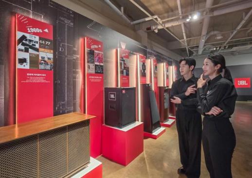 Samsung turns up the volume on its audio heritage SEOUL, October 21 (AJP) - Samsung Electronics excels at making memory and smart devices for the hand, home and office, and screens big and small. But one element of its sprawling electronics empire called for a richer pedigree: sound. Its biggest acquisition to date brought that heritage into the family. The $8 billion deal to buy Harman International completed in March 2017 added the storied American audio brand JBL alongside a major automotive electronics business. Posh Britain audio brand Bowers & Wilkins joined the family last year through Harman’s purchase of Sound United. Their adoptive Korean parent has thrown a birthday bash for the family’s elder members as JBL turns 80 and Bowers & Wilkins marks its 60th anniversary. “Sound Legends,” running from Oct. 24 to 31 at Project Space Line in Seoul’s Gangnam district, brings together vintage speakers, recording equipment and contemporary audio devices to trace how sound developed for cinemas and studios found its way into homes and everyday life. “This year we're celebrating three very important milestones — the 60th anniversary of Bowers & Wilkins, the 80th anniversary of JBL and ten years being part of the Samsung family,” David Glaubke, a communications director at Harman International, told reporters Wednesday. The Samsung milestone dates from the acquisition announcement; the transaction closed the following March. The exhibition reaches back much further, opening with a Jackson-Bell radio from 1929 fitted with a speaker developed by Lansing Manufacturing, the company audio engineer James B. Lansing founded in 1927. Lansing went on to establish JBL in 1946, giving the company his initials. Its early work in cinema and professional sound laid the foundations for a business that would eventually reach living rooms around the world. One of the exhibition’s centerpieces is the JBL Paragon, a sweeping wooden stereo speaker that looks as much like a finely crafted sideboard as a piece of audio equipment. Introduced in 1957, according to the exhibition guide, it housed the left and right channels in a single cabinet. Each required roughly 100 hours of skilled woodworking, and only about 1,000 were made before production ended in 1983. The scale and craftsmanship belong to an era when a sound system could command an entire room. A more compact milestone followed in 1970 with the L100 Century, a home speaker derived from JBL’s 4310 studio monitor. Its distinctive foam grille helped make it one of the brand’s most recognizable consumer products, bringing a piece of the recording studio into the home. The display continues through to the JBL Summit K2, a high-end speaker being shown in South Korea for the first time, alongside portable speakers and headphones. Together, the exhibits chart the journey from imposing cabinets built for dedicated listening to devices that carry music almost anywhere. On another floor, Bowers & Wilkins tells a parallel story with a distinctly British accent. Founded in England in 1966, the company built its reputation on reproducing recordings as faithfully as possible. Its speakers have been used at London’s Abbey Road Studios, where generations of musicians and producers have recorded and mixed their work. Its most arresting exhibit is the Nautilus. Introduced in 1993, the speaker resembles a sea creature, with a shell-like body and tapered tubes extending behind its drivers. The unusual form serves an acoustic purpose: controlling unwanted sound from the rear of the drivers. More than three decades later, the model remains in production on a made-to-order basis, according to the exhibition guide. Visitors can also listen to the latest 800 Series Diamond D5 speakers, whose synthetic diamond dome tweeters are designed to reproduce high frequencies with greater precision. For Samsung, the display of audio history also showcases a business that has grown substantially under its ownership. Harman’s reported annual revenue rose from 7.1 trillion won in 2017 to 15.8 trillion won in 2025, according to Samsung, while operating profit reached a record 1.5 trillion won last year. The comparison begins with the year Samsung completed the acquisition. The portfolio has grown, too. Harman’s $350 million acquisition of Sound United last year brought Bowers & Wilkins, Denon and Marantz into the group, extending its reach across premium home audio. Samsung plans to explore further applications for Harman’s audio technologies across smartphones, televisions and soundbars, although it has not specified products or launch dates. The Seoul exhibition forms part of a global JBL anniversary tour that has visited Amsterdam, Los Angeles, New York and Tokyo. For a company more readily associated with memory chips and Galaxy phones, it offers a different kind of family portrait: wooden cabinets, sculptural speakers and decades of engineering devoted to what comes out of a device, rather than what appears on its screen. 2026-10-21 18:02:48
 -
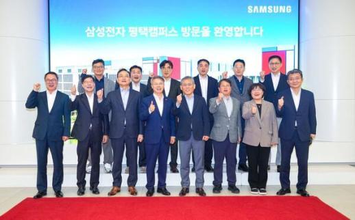 Samsung's chip plans put schools, roads and water on Gwangju's agenda SEOUL, October 21 (AJP) - Samsung Electronics has outlined infrastructure needs for a planned semiconductor cluster in Gwangju, including international schools, wider roads and recycled wastewater facilities, according to the local government Wednesday. The requests came during a visit by officials from the Gwangju-Jeonnam Special Metropolitan Government to Samsung's Pyeongtaek semiconductor campus on Tuesday. Samsung representatives stressed the need for international or foreign schools to accommodate employees' families, roads with at least eight lanes to handle factory traffic and materials shipments, and facilities to reuse treated wastewater for chip production, according to the city. The local government plans to review the requests and consider incorporating them into infrastructure plans for the proposed semiconductor complex. Semiconductor fabrication plants require vast quantities of ultrapure water to clean silicon wafers during manufacturing, making a reliable water supply and wastewater treatment capacity essential to large-scale chip production. The discussions highlight the extensive supporting infrastructure required for large-scale chip manufacturing, where access to water, transportation and skilled workers can be as critical as the factories themselves. 2026-10-21 16:07:14
 -
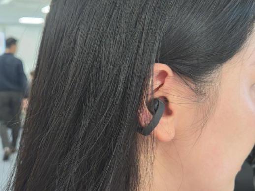 Loose fit, firm grip: Hands on Samsung's first clip-on Galaxy earbuds SEOUL, October 20 (AJP) - Samsung Electronics’ latest Galaxy earbuds perched comfortably around the ears instead of plugging into them. A few jumps and jogging motions later, they were still there, intact with lighter feel. That was the main takeaway from trying the Galaxy Buds On at Samsung’s media briefing in central Seoul on Tuesday. They felt loose enough to raise doubts about their grip, but soon became so unobtrusive that it was easy to forget you had them on. For people who wear earbuds almost as an extension of their bodies, the difference is immediately noticeable. There is no tip nestled inside the ear canal. Instead, the buds clasp the outer ear, leaving the canal open to the world beyond the music. Samsung is pitching that balance to listeners who want a soundtrack to their day while keeping an ear on conversations and their surroundings. Unveiled on Oct. 1, the Galaxy Buds On will go on sale in South Korea on Oct. 27 for 299,000 won. The only color is black. During the hands-on session, the familiar snugness of in-ear buds gave way to a lighter, less enclosed sensation. The fit suggested freedom to move; the jumping and jogging showed that freedom did not necessarily come at the expense of stability. The buds held their position without the wedged-in feeling of conventional earbuds. That was encouraging, though a few movements in a briefing room are a modest test. A long commute or a sweaty workout could tell a different story about pressure, comfort and grip. Getting that balance right across different ear shapes was a central development challenge, Samsung said. A shape-memory alloy band links the speaker and battery sections, flexing to accommodate the ear. Behind that simple-looking curve is what Samsung calls 4D computing-based AI optimization, used to simulate component arrangements and fine-tune how pressure is distributed. “Recently, more users have wanted to enjoy content while also hearing their surroundings,” said Nam Hyun-jung, a member of Samsung’s MX wearable product planning group, according to briefing materials. An open ear, however, gives the sound more room to wander. With the speaker sitting farther from the canal, bass can lose its punch and music can spill beyond its intended audience. Samsung has fitted each earbud with two identical woofers, branded TwinBoost speakers, to bolster the low end. Sound-leakage reduction technology is intended to keep more of the listening experience private. The company nevertheless acknowledged that nearby people may still hear some audio, depending on the volume, the wearer’s ear shape and the surrounding noise. How much bass reaches the listener—and how much music reaches the next person—will need a longer test in quieter and busier settings. The earbuds can also adjust playback volume as ambient noise changes. Company representatives said the automatic adjustment has a ceiling, rather than endlessly chasing a louder environment with louder music. For calls, Samsung says three microphones, a voice vibration sensor and machine-learning software help pick the wearer’s speech out of background noise. The vibration sensor assists with voice pickup; it does not mean music is delivered through bone conduction. Several other features aim to take the small frictions out of daily use. There is no need to inspect the buds for left and right markings before putting them on. They automatically assign the audio channels according to which ear they occupy. Voice commands, head gestures and quick voice recordings are designed to keep the phone in the pocket more often. When paired with a compatible Galaxy device, the buds can also summon Google’s Gemini Live for spoken conversations. Some functions depend on the connected device and software version. The design is less accommodating when it comes to personal taste. Something worn so visibly around the ear invites a choice of finishes, but buyers will have to settle for black. For now, though, the fit makes the strongest case. The Buds On felt as though they were taking a lighter hold, yet jumping and jogging failed to shake them loose. They passed that first test of staying on. Whether they remain something the wearer wants to keep on for hours is the question for the next outing. 2026-10-20 15:33:25
 -
 Investors question AI boom, but Samsung's feud over windfall deepens SEOUL, October 19 (AJP) - Investors are moving on from Samsung Electronics amid quibbles over whether the AI boom is past its heyday, but inside the company employees are still fighting over their share of the profits it has already delivered. The simmering dispute has escalated into allegations of a physical confrontation between security personnel and a union leader representing disgruntled consumer electronics employees, prompting calls for an apology from Chairman Lee Jae-yong. “What we received was not dialogue but physical violence,” Samsung’s Donghaeng union said at a press conference outside the company’s Seocho office on Monday afternoon, referring to an Oct. 16 encounter at its Suwon campus. The union alleges that its leader, Son Yong-ho, was injured when security personnel restrained him as he approached a vehicle it identified as Lee’s to seek direct talks with the chairman. Son was pushed against a wall and fell, striking his head on the floor, according to the union. It said he required hospital treatment for bruising, dizziness, concussion-like symptoms and a temporary loss of memory surrounding part of the encounter. Son appeared at Monday’s press conference in hospital clothing and said he had hurried to the event by taxi. Asked about his admission and discharge dates and his diagnosis, union officials declined to provide details, citing personal privacy. The union said it had confirmed that Lee emerged from the vehicle after it moved away. Samsung declined to comment on the encounter. The union demanded a personal apology from Lee, an investigation and action against those responsible, along with direct dialogue with employees. It said repeated requests to meet the chairman had been rejected and discussions with human resources officials and senior management had led nowhere. For now, the union said it was seeking an apology and accountability rather than pursuing legal action. The confrontation has brought Samsung’s widening internal divisions into public view just as investors begin questioning the longevity of the windfall behind them. Samsung estimated third-quarter operating profit at a record 107.4 trillion won (about $80 billion), nearly nine times the year-earlier figure, with an operating margin above 55 percent. Cumulative operating profit through September reached 254.13 trillion won, about 10 times its full-year earnings in 2025. Yet the extraordinary earnings have offered little protection against the stock market’s reassessment of AI. Concerns over the cost of financing AI infrastructure and the returns on that investment have unsettled technology shares, challenging expectations that the spending boom will keep delivering ever-larger gains for chipmakers. Samsung shares have lost about 21 percent this month. They recovered 3 percent Monday. Inside the company, the argument is over how the gains already made should be distributed. The Device Solutions division, which houses Samsung’s semiconductor business, has benefited from surging demand for AI memory chips. Employees in the Device eXperience division, which makes smartphones, televisions and home appliances, argue that the resulting compensation gap overlooks their contribution to the same company. The company’s largest union estimates that a memory-chip employee with a base salary of around 80 million won could receive about 750 million won in pretax bonuses, including existing annual incentives, if full-year operating profit reaches 370 trillion won. Device eXperience employees are excluded from the new semiconductor bonus scheme. They were instead allocated 6 million won worth of shares alongside their existing incentives, fueling resentment over the disparity. The dispute predates the latest market rout. But the reversal has left management confronting two very different demands: investors want reassurance about future profits, while employees want a greater share of past gains. Samsung must now settle the argument over the rewards of the boom before the divisions it has exposed outlast the windfall itself. 2026-10-19 18:14:22
 -
 Korean chipmakers reassure they can stay ahead of CXMT SEOUL, October 16 (AJP) - South Korean chipmakers claim they are in a different league from ChangXin Memory Technologies (CXMT), an Anhui-based Chinese memory maker little known outside the industry until its spectacular Shanghai stock-market debut in July. They find themselves having to reassure questioning investors as the Chinese challenger pushes deeper into server DRAM, promising a product using a novel, denser memory-cell design called 4F² by year-end. Song Jae-hyuk, the deadpan chief technology officer of Samsung’s chip division, was bombarded with questions about the feat at Samsung’s SEDEX 2026 booth in Seoul on Oct. 14. He stoically acknowledged that Samsung, too, had been researching 4F² DRAM — a rare moment in which the Korean giant found itself answering questions about a Chinese underdog’s apparent head start. Samsung Electronics shares plunged more than 10 percent and SK hynix lost 13 percent Thursday. Are investors overreacting? For now, experts caution against mistaking a prototype for a commercial breakthrough. But they also acknowledge that China’s faster-than-expected ascent in a DRAM market long dominated by the two Korean chipmakers and Micron cannot be dismissed, particularly given its restricted access to advanced chipmaking equipment. “If it is true that they have made a working die or a prototype, that alone is surprising,” Kim Deok-kee, a professor at Sejong University, said. A functioning CXMT prototype would be a significant achievement if confirmed, he said, because the design represents a next-generation technology that established memory manufacturers are also pursuing. Whether the design translates into a commercially competitive product remains an open question. Samsung and SK hynix are moving ahead with their own development, leaving the eventual pecking order far from settled. The 4F² designation describes the area occupied by a memory cell. At the same minimum feature size, it represents a cell footprint one-third smaller than a 6F² layout, potentially allowing more memory cells within a given area. Kim described the move toward smaller cells as a shared industry direction, rather than an entirely separate technological path pioneered by one company. The difficulty lies in fitting the components into a more compact structure while making the design work as a product. A prototype can demonstrate that a concept functions. It does not, by itself, establish manufacturing yields — the proportion of usable chips produced — or show how consistently a supplier can deliver products meeting customer requirements. Chinese manufacturers appear to be making an aggressive push into next-generation technologies, Kim said. Even so, announcing progress on a particular structure should not be treated as proof of leadership in finished products. A source close to Samsung Electronics told AJP that the company was working toward mass production of DRAM using the design around 2028. “We are working quietly, building a solid foundation,” the source said, adding that the products in which the technology would be used had not been finalized. SK hynix separately confirmed to AJP that it was developing the technology. The company had outlined its plans for 4F² DRAM as early as June 2025, when Chief Technology Officer Cha Sun-yong presented a long-term technology roadmap. At the time, Cha identified 4F² vertical-gate technology and 3D DRAM as key areas of development to overcome the limitations of conventional memory scaling. SK hynix also said it was exploring wafer-bonding technology to improve cell efficiency and electrical performance. Ahn Ki-hyun, an official at the Korea Semiconductor Industry Association, said the information available was insufficient to quantify the gap between CXMT and its Korean competitors. “We have to test them under the same conditions to make a comparison,” Ahn told AJP. Assessing CXMT’s competitive position based solely on its claims was nearly impossible without examining an actual product, he said. A meaningful comparison would require commercially available products that could be purchased and tested. Customer adoption will provide another test of how far development progress translates into a competitive business. Apple Chief Executive John Ternus told TIME in an interview published Thursday that memory shortages warranted considering all supply options. His comments came amid reports that Apple was testing Chinese-made memory, but did not confirm a commercial supply agreement. Any evaluation of memory for consumer devices would also be separate from validation of CXMT’s proposed server products. For CXMT, the next milestones are more concrete than a claim of progress: a product that can be independently assessed, manufactured consistently and accepted by customers. For the Korean chipmakers, the challenge is to prove that being first to announce a new design is one thing — and delivering it reliably at scale is another. Shares of Samsung Electronics and SK hynix staged a modest recovery Friday, closing up 3.6 percent and 1.2 percent, respectively. 2026-10-16 17:08:05